
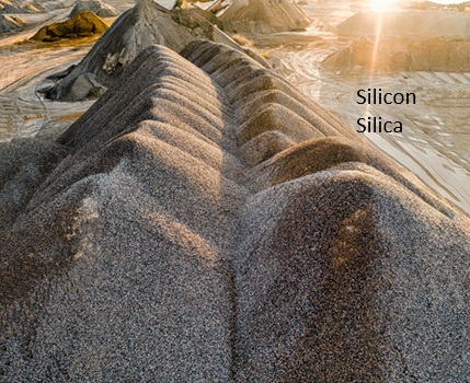
Silicon represented by symbol Si is the second most abundant element by weight in the earth’s crust. About a quarter of the mass of earth’s crust is made up of Silicon. It is present all around us in rocks, sands, and soil in the form of silica and silicates. Silica and silicates are compounds containing Silicon and Oxygen. Silicon is present in substances that we use in our day to day lives – in ceramics, porcelain plates and dishes, glass containers and utensils and in today’s microelectronic devices such as calculators, personal computers, and mobile phones. Without Silicon, it would not have been possible to have handy microelectronic devices and personal computers. In this blog, I discuss the properties of Silicon that makes it suitable for its applications. I try not to delve much into scientific aspects and thereby make this blog comprehensible for all readers regardless of their background in science.
General Properties of Silicon
Silicon is in Group 4 of the periodic table. It is classified as a metalloid, i.e. it exhibits the properties of both metals and non-metals. As a metal, it is shiny, has a metallic look, and forms a well-defined crystal structure. As a non-metal, it crumbles and does not form sheets like metals, it (pure silicon) does not conduct electricity on its own. It has atomic number 14, i.e. it has 14 protons and 14 electrons with electronic configuration 1s22s22p63s23p2. It has 4 valence electrons. It is present in minerals silica and quartz as Silicon dioxide (SiO2). Silicon is extracted from silica and quartz by reduction with Magnesium metal.
SiO2 + 2Mg -> Si + 2MgO
Extraction of elemental Silicon from naturally occurring Silica is important as only pure Silicon is used in the manufacture of microelectronic devices. Extracted Silicon is purified to prepare Silicon crystals which are used to make Silicon chips.
Three companies produce Silicon in the United States. On a global level, China is the top producer of Silicon followed by Brazil, Norway, France, Australia, Russia, Canada, and other countries. There are adequate resources for making Silicon metals and alloys around the world.2
Properties of Silicon and its applications
Silicon as a Network Atomic Solid
Before discussing the properties and applications of Silicon, it will be helpful to know about the bonding and structure of Silicon and Silica. Bonding has a profound effect on physical and chemical properties of elements and compounds. The physical and chemical properties again have an effect on their chemical reactions. The structure and properties of Silicon and Silica change at various temperatures and with addition of impurities/other elements on them. This behavior makes it useful for its various applications.
Silicon and Silica form what can be called as network solids. Silicon when purified into a crystal forms a tetrahedral structure with one Silicon atom bonded to 4 other Silicon atoms in the case of Silicon crystal and one Silicon atom bonded to 4 other oxygen atoms in the case of Silica. Disruption or modification of these network solids structure changes its properties and thereby its applications. Hence it is important to know about the network atomic solid structure of Silicon and Silica.
Silicon is in the same Group 4 as Carbon, the element which forms the most number of compounds in this earth. Being under the same Group and just below Carbon in the periodic table, we would expect Carbon and Silicon to have similar structures. But they have very different structures. Carbon can form long chains of compounds with Carbon-Carbon bonds but Silicon cannot form chains as long as Carbon. The larger size of Silicon Si restricts the length of the chains. Having a bigger atomic radius 1.17A°(Angstrom) compared to C with atomic radius 0.77A°(Angstrom), Silicon forms shorter chains. Pure Silicon exhibits a network tetrahedral crystal lattice structure with each Si-Si bond angle of 109°. Such pure Silicon solid is prepared as a thin wafer sheet upon which several printed circuits are etched to create diode transistors for microelectronic devices.
Here is a schematic representation of Silicon network atomic solid structure.
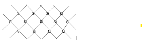
The formation of such a network solid crystal lattice is necessary in order for Silicon to be doped with impurities. Doping is important for making Silicon useful for application as a semiconductor in microelectronic devices.
Next coming to the most common form of Silicon which is Silica, ie. Silicon dioxide (SiO2) – Silica is a solid whereas Carbon dioxide (CO2) is a gas. This is because of the way by which the Silicon Si and Carbon C are bonded with Oxygen O.
CO2 has a linear structure represented by O=C=O. Carbon forms a double bond with Oxygen on either side and is a linear molecule as shown by a bond angle of 180°. This is because of the similar size of the two atoms C and O leading to effective sideways overlap of the orbitals containing the valence electrons. Remember, an orbital is an energy level or energy band where there is maximum probability of finding the electrons. On the other hand, SiO2 is a solid where Si and O are not bonded by a double bond but by a single bond because Si has a bigger atomic size than O. Because of the difference in sizes, there is no sideways overlap as in Carbon and hence there is no double bond. Instead, Si forms a strong single bond with oxygen. The bonding in SiO2 cannot be represented by a single unit of SiO2 but by a network of units of SIO2. Below is a schematic structure of SiO2:

A single Silicon forms 4 bonds with Oxygen and the Si:O ratio is 1:2. Each Silicon atom is at a tetrahedral arrangement, i.e. 108° bond angle between Si and O. The above is just a schematic representation to show SiO2 is represented as a network of SiO4 units of Silicon atoms bonded with oxygen atoms. Although the empirical formula for Silica is SiO2, the structure is based on a network of SiO4 tetrahedra with shared oxygen atoms rather than discrete SiO2 molecules. The differing abilities of carbon and silicon to form π bonds with oxygen have profound effects on the structures and properties of CO2 and SiO2. This type of solid structure is called as Network Atomic Solid. This solid structure paves the way for some of the applications of Silica such as in glass formation and ceramics.
Band Gap Model
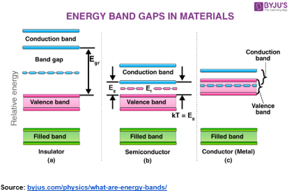
The Band Gap model or Molecular Orbital (MO) model assumes electrons travel around the crystal in molecular orbitals formed from the valence atomic orbitals of the atoms. (Remember, an orbital is an energy level or energy band where there is maximum probability of finding the electrons.). As per this model, the valence band orbital is the highest occupied molecular orbital(HOMO) in the atom and it is occupied by valence electrons. Higher in energy level than the valence band orbital or HOMO is the conduction band or Lowest Unoccupied Molecular orbital (LUMO). The difference in the energy or distance between the valence band and conduction band is called the Band Gap. Band Gap is measured in Electron Volt eV.
In an insulator like Graphite, the Band Gap is very high in the order of 5eV. At this distance, the electrons cannot travel from the valence band to the conduction band and hence there is no flow of current. In metal, the band gap is very small or there is no separation of the two bands. The two bands overlap and there is always a flow of electrons in the metals. Both these behaviors are not suitable for use in microelectronic devices.
In a semiconductor, the Band Gap is at an appropriate level where there is no flow or negligible flow of electrons at normal conditions. However, when external thermal energy or dopant is added to the crystal, electrons move from valence band to conduction band. They do not conduct electrons by themselves but when an external factor is applied it starts conducting electrons and hence is called a semiconductor.
Thus the postulates of the Band Gap Model satisfy the observed electron conducting behavior of metals, insulators, and semiconductors.
Selected applications of Silicon
Semiconductor
As mentioned before, Silicon is a semi-metal or metalloid. It shows both properties of metal and non-metal. As a metal, it is shiny, has a metallic look, and forms a well-defined crystal structure. As a non-metal, it crumbles and does not form sheets like metals and it does not conduct electricity on its own.
Pure silicon does not conduct electricity. But when some impurities are added, it conducts electricity. It is a semiconductor because its conduct of electricity (i.e. movement of electrons) is in between that of a conductor and insulator. At normal conditions, it does not conduct electricity like an insulator. However, when some impurities are added, it conducts electricity like metals/conductors. This property of Silicon as a semiconductor comes in extremely handy for designing microelectronic devices as we can manage through switches the flow of current on Silicon chips. With the Band Gap Model, we can provide a satisfactory explanation of Silicon behavior as a semiconductor.
Silicon has a Band Gap at 1.1eV which is at the appropriate level for using it as conductor for microelectronic devices. We are aware that Silicon has 4 valence electrons, i.e. 4 electrons that can take part in bonding. The 4 valence electrons are in the valence band at normal temperatures. However, when a dopant from Group V or Group III is added, the electrons or holes created respectively allow for the flow of electrons from valence band to conduction band or flow of holes from conduction band to valence band. This flow of current carriers is controlled through switches by applying suitable voltages. Thus the flow of current under controllable conditions makes Silicon an extremely useful element in microelectronic devices.
In order to use Silicon in microelectronic devices, Silicon is first purified to form crystals. It is then made into wafers. Printed circuits with external switches are etched on these wafers to manufacture microelectronic devices.
Glass
While crystal is an ordered and repeating arrangement of atoms on a solid network, amorphous solids are random and disordered arrangements of atoms. When Silica is heated above its melting point (about 1600℃) and cooled rapidly in the presence of substances such as Sodium carbonate, the crystalline form of Silica gets disturbed and forms an amorphous solid called Glass. When additives are added, we get different types of glasses. Different types of additives are added in different ratios based on the desired end product. These additives intercalate between the Silicon and Oxygen atomic solid network (described above) to get different types of glasses with different strengths and properties. For example:
- Adding Boric oxide gives borosilicate glass. This borosilicate glass expands and contracts little under temperature changes and hence is useful for labware and cooking utensils
- Adding Potassium oxide produces a type of glass that is hard and that can be made into different shapes needed for eyeglass and contact lenses
- Adding Aluminum oxide makes the glass very brittle and aluminosilicate glass is used as cookware
Ceramics
Ceramics are made from clays which are silicates (i.e. compounds containing Silicon and Oxygen with some positively charged particles to balance charges and to make it a neutral molecule). The silicates are hardened by firing at high temperatures. Even though they are not metals, the ceramics get so hardened that they become strong, brittle, and resistant to heat as metals when heated. Once formed, the shape of ceramics cannot be changed. This is in contrast to glasses where glasses can be melted and re-melted as often as desired.
To understand why clays become so hard when heated, we have to know about the structure of clays. Clays are a mixture of Potassium oxide, Aluminum oxide, Sodium oxide and Silicates. The oxides are intercalated in silicate structures. Clays occur naturally in rocks. When these rocks weather by the action of water and carbon dioxide, clays become a mixture of Aluminum oxide and Silicates. The layers of aluminum oxide and silicon oxide slide over one another giving its plasticity. When the clay gets dried, they get tightly interlocked, which gives its brittleness. When the remaining water is driven off by heating, it gets further tightly interlocked making it permanently hard without allowing for any re-shaping of the structure.
Summary
I discussed the general properties of Silicon, the Network Atomic Solid structure and bonding in Silicon and Silica, and the Band gap model. The Network Atomic Solid structure of Silicon and Silica helps to explain the significance of bonding, the effect of doping on Silicon and the formation of ceramics on Silicates. The Band Gap model serves as an effective postulate to explain the conducting behavior of semiconductors. Further, we saw that Silicon’s property as a metalloid and semiconductor comes handy in the manufacture of microelectronic devices. Before the invention of Silicon chips, computers and electronic devices were made with vacuum tubes which were larger in size. Thus, the invention of Silicon chips had a major breakthrough in the manufacture of handheld microelectronic devices that we have got so used to in this digital age.
Silicon has been an important element at every period of human history – from ceramics to pottery to fancy utensils to glasses to electronic chips. In this blog, I focused on Silicon, its bonding, structure, properties and its applications in glass-making, ceramics, and microelectronic devices. In the subsequent blogs, I will discuss the doping elements, the choice of different doping elements based on the end-product, and the formation of NPN junctions in Silicon. The formation of NPN junctions is the basis of the printed circuit that is etched on Silicon chips. The printed circuits conduct electricity and pave the way for designing various microelectronic devices.
Bibliography
1. Chemistry, Steven S. Zumdahl, Second Edition, D. C. Heath and Company
2. Mineral Commodities Summary 2026, US Geological Survey
Image courtesy: Photo by Tom Fisk from Pexels: https://www.pexels.com/photo/sand-and-gravel-hills-11160727/


Leave a Reply